The electronics industry is in trouble. Unless someone develops a bright idea soon, the long assembly line of progress that has produced ever smaller, faster, cheaper, more powerful computers, cell phones and other electronic devices will likely short circuit and grind to a halt by 2020. Experts predict the limits of current semiconductor technology will be reached that year.
Much of the innovation nurtured into businesses at Innovation Park, the joint ND/South Bend high-tech business incubator located just east of Eddy Street Commons, will likely address this problem. And many of the bright ideas behind all that innovation are likely to come from the MIND at ND.
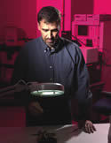
For the past 50 years, electronics has been based on the same technology, the transistor, explains Alan Seabaugh, a Notre Dame professor of electrical engineering who is the new director of the Midwest Institute for Nanoelectronics Discovery (MIND). “We’ve just been making them smaller and smaller, but as they’ve shrunk in size they work less and less well, leaking heat and current. So now we’ve been given the opportunity to find the next technology.”
The MIND is a new collaborative research effort headquartered at Notre Dame involving engineers and scientists from ND, Purdue, the universities of Illinois, Michigan, Texas-Dallas and Penn State as well as several national laboratories. Initially unveiled in March as the Midwest Academy for Nanoelectronics and Architectures, the name was changed in May when it was discovered the MANA acronym already had been trademarked by another group.
Notre Dame was one of 30 institutions that sought to acquire the research unit, one of four regional centers established by the Nanoelectronics Research Initiative of the Semiconductor Research Corporation, a consortium of semiconductor manufacturers. Key to the University’s successful bid was the state-of-the-art Stinson-Remick Hall, now under construction.
The building, which will house MIND and Notre Dame’s Center for Nano Science and Technology as well as the Notre Dame Energy Center, boasts such cutting-edge features as a 10,000 square-foot “clean room” with air filtration 20,000 times purer than natural air for fabricating nanoscale semiconductor devices, which may be the size of atoms or smaller. Additionally, the new engineering hall has been designed to minimize building vibration, which is important for the delicate manipulations involved in nanotechnology.
Initially, Seabaugh says, MIND will focus on a variety of projects in four main areas. In one approach pioneered at Notre Dame and known as quantum-dot cellular automata (QCA), a number of researchers will examine the feasability of employing tiny, electron-confining structures called quantum dots. Using microelectronic techniques, these “caged electron” cells can be lined up to form wires, switches or other computer logic devices. Researchers estimate a 4-square-centimeter QCA chip could contain up to 1 trillion devices compared to the 2 billion transistors in the most advanced conventional chip.
Another approach to be explored at MIND involves finding ways to employ the quantum-mechanical effect to make more efficient switches. “Tunneling” is an effect observed at the nanometer level in which an electron is able to pass through an energy barrier if it is sufficiently thin. An electric field can be used to vary the barrier’s thickness and control electron flow.
A third thrust of the new research center will involve designing the most efficient and novel ways of connecting these new generation semiconductor devices.
Writing the future
The director of MIND, however, is especially enthusiastic about the fourth area of study which—as strange as it may seem—involves an exotic form of pencil lead that just might write the future of the electronics industry.
“Graphene is a newly discovered form of graphite; it is a unique material, the thinnest known to humankind,” says Debdeep Jena, a Notre Dame assistant professor of electrical engineering who is investigating the material. “Essentially, it is a sheet of carbon atoms only 1-atom thick, bonded together in a honeycomb arrangement.”
That quality makes it capable of much more than traditional transistors, he says. “Since it’s only 1-atom thick it is effectively transparent, and therefore you can place it on something that bends. Since microprocessors need not be rigid any more, it ushers in the era of extremely powerful, flexible electronics.”
As innovative as that may be, it represents just one more evolutionary shrinking of the traditional transistor. What really excites Jena is that graphene could usher in a true electronics revolution. In theory, he says, the unique behavior of graphene electrons makes possible superior devices that could replace the transistor as the fundamental building block of electronics.
Graphene electrons behave like light waves, unlike the “point” behavior of classical electrons, the ND engineer explains. Therefore, it may be possible to produce products that have the advantages of both light-based technologies, such as the laser photonics behind DVD players, and the classic electron-based devices used, for instance, in computers and cell phones. Photonic cirucits now are relatively large scale, Jena says, but graphene may allow photonic-like circuits at incredibly small scale.
For all these reasons, graphene seems to be the ideal next-generation electronic material. Jena and his colleagues are now trying to determine the maximum amount of electric current that can be pushed through the substance. This is important to know, he says, because the greater the current moved, the faster the switch—and the faster the computer or other electronic device will work.
The new institute had its kickoff meeting in early June, at which time researchers from the four main areas outlined the state of the art in their fields and presented their research plans to one another and representatives of industry.
Before any graphene-based businesses migrate from the researchers to the entrepreneurs in Innovation Park, a huge array of technical problems must be solved. However, with some luck and the many minds of the MIND working, the solutions may come quicker than anyone knows.
_Alan Seabaugh photo by Matt Cashore _